SMT Line
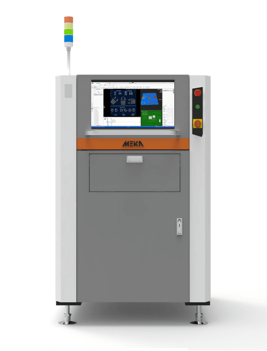
MEKA-S3 3D Solder Paste Inspection (3D SPI)
S-Series 3D SPI equipment featuring self-developed head control driver card, 4-segment SMD LED light source, and 3000-level precise light control. 3D solution algorithm optimized for scene, uses white light projection, compatible with panels of different colors. Available in S3/S3 Pro/S3 Pro Max/S3 Ultra with 12MP~25MP cameras.
Key Specs
ModelsMEKA-S3 / S3 Pro / S3 Pro Max / S3 Ultra
Camera12MP / 18MP / 25MP / 21MP
Pixel Size3.5um~20um
Inspection Speed0.35s / 0.45s / 0.45s / 0.55s per FOV
Max PCB (Single-lane)50×50 ~ 510×460mm
Max PCB (Double-lane)50×50 ~ 510×580mm (Single Mode) / 50×50 ~ 510×320mm (Dual Mode)
DLP StandardSingle-Direction Moiré Pattern Projection
DLP OptionalBi-Directional Moiré Pattern Projection
See full specifications below
Applications
SMT solder paste print quality inspection
Solder paste volume/height/area/offset measurement
Solder bridging detection
Stencil aperture blockage detection
Printing process closed-loop feedback optimization
Detailed Description
Overview
The MEKA-S3 is CTW's self-developed 3D Solder Paste Inspection (3D SPI) system in the S-Series. It features a self-developed head control driver card with high-efficiency dual magnetic circuit 4-segment SMD LED light source and 3000-level precise light control.
Key Advantages
Self-developed 3D Algorithm
- Scene-optimized 3D solution algorithm
- White light projection technology
- Compatible with panels of different colors
- High solution stability
High-Precision Inspection
- Height accuracy ±1um
- Up to 25MP camera resolution
- Pixel size down to 3.5um
Multiple Models
| Model | Camera | Speed |
|---|---|---|
| MEKA-S3 | 12MP | 0.35s/FOV |
| MEKA-S3 Pro | 18MP | 0.45s/FOV |
| MEKA-S3 Pro Max | 25MP | 0.45s/FOV |
| MEKA-S3 Ultra | 21MP | 0.55s/FOV |