Introduction
In the fast-evolving landscape of electronics manufacturing, Automated Optical Inspection (AOI) remains a cornerstone of quality control on SMT and DIP lines. From post-reflow solder joint screening to odd-form component verification, AOI directly determines the quality floor and operational efficiency of every production line. For over a decade, 2D AOI has served as the industry workhorse, leveraging mature planar imaging and pattern-matching algorithms. However, as consumer electronics and automotive electronics continue to demand smaller form factors and higher-density packaging, traditional 2D inspection is encountering increasingly critical blind spots.
Industry data shows that 3D AOI's share of the global AOI market has grown from under 30% in 2020 to over 55% in 2025, and the momentum is accelerating. From both a technology evolution and market demand perspective, the question is no longer whether 3D AOI will replace 2D AOI, but how quickly the transition will be completed.
The Bottlenecks of 2D AOI
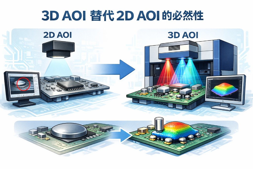
2D AOI captures planar images from single or multiple camera angles and applies grayscale, color, and edge-detection algorithms to identify defects. While effective under specific conditions, this approach has fundamental structural limitations:
The Missing Height Dimension
A 2D image is inherently a projection that discards all Z-axis information — solder height, volume, and coplanarity are invisible. Defects such as insufficient solder, excess solder, tombstoning, and joint collapse must be inferred indirectly from grayscale variations and shadow cues, leading to accuracy limitations where false calls and escapes are difficult to reduce simultaneously.
Blind Spots for 3D Defects
For complex three-dimensional defects like bridging, cold joints, solder balls, and QFN/BGA pad-level coplanarity, a single top-down view provides severely insufficient information. On high-density HDI boards and mixed-technology assemblies, component shadowing and specular reflection further amplify these blind spots.
Insufficient Process Adaptability
Different PCB base colors (green, black, white solder mask), surface finishes (HASL, OSP, ENIG), and paste brands significantly alter image reflectance and contrast. 2D algorithms frequently require per-line or even per-batch parameter tuning, consuming substantial engineering effort and driving up maintenance costs.
Broken Data Loop with 3D SPI
An increasing number of SMT lines have deployed 3D SPI (Solder Paste Inspection) at the print stage, precisely measuring paste volume, height, and offset. If post-reflow inspection remains 2D, the "paste volume to joint height" data chain is broken — effective process closed-loop analysis and root-cause tracing become impossible, and the value of 3D SPI data is significantly undermined.
The Core Advantages of 3D AOI
3D AOI retains full 2D planar inspection capability while adding height information through structured light projection, Moire fringe, or phase-shift techniques — enabling a fundamental shift from "guessing defects from images" to "measuring defects with data."
True Height and Volume Measurement
3D AOI directly measures solder joint height, volume, and coplanarity, providing quantitative pass/fail values for insufficient solder, excess solder, tombstoning, and collapse — replacing experience-based grayscale thresholds. Inspection criteria can be defined to micrometer precision, and escape and false-call rates can be reduced by 40%–60% compared to 2D.
More Complete Defect Coverage
With 3D data, the height profile of bridges, the wetting angle of cold joints, and the coplanarity of QFN/BGA packages can all be quantitatively defined and reliably detected. For 0201 and 01005 ultra-small passives and sub-0.3mm pitch fine-pitch devices, the advantage of 3D inspection becomes even more pronounced.
Full-Process Data Closed Loop with 3D SPI
When a line is equipped with both 3D SPI and 3D AOI, end-to-end 3D data traceability from print to post-reflow becomes possible: SPI records paste quality, AOI records post-solder quality, and both are correlated through SPC (Statistical Process Control) to rapidly pinpoint root causes of process drift, enabling predictive maintenance and continuous improvement.
Greater Process Robustness
Geometric features such as height and volume are far less sensitive to PCB color and surface reflectance than grayscale features. 3D AOI can reduce parameter tuning workload by over 50%, making it especially suitable for high-mix, low-volume, and rapid-changeover flexible manufacturing lines.
Industry Trends: The Replacement Is Accelerating
Driven by Advanced Packaging
The high-volume adoption of SiP (System-in-Package), PoP (Package-on-Package), Mini LED, and Micro LED brings higher solder joint density and more stringent inspection requirements. In these applications, 2D AOI simply cannot meet the demands — 3D inspection is a necessity.
Escalating End-Market Requirements
Automotive electronics follow IATF 16949 and zero-defect targets; medical electronics require full-process traceability; industrial and telecom equipment demand long-term reliability. These industries' quantitative inspection requirements are compelling production lines to upgrade from 2D to 3D.
Improving TCO (Total Cost of Ownership)
3D AOI hardware costs have declined steadily over recent years, while the total savings from reduced customer returns due to fewer escapes, lower rework labor from fewer false calls, and shorter programming time have brought TCO to parity with — or better than — premium 2D solutions. For mid-to-high-end lines, the payback period for 3D AOI is typically 12–18 months.
Conclusion
From the standpoint of technological evolution and market demand, the comprehensive replacement of 2D AOI by 3D AOI has become a clear inevitability. It resolves the fundamental shortcoming of height detection while demonstrating irreversible advantages in data closed-loop capability, process adaptability, and total cost of ownership.
In SMT and DIP inspection, the MEKA 3D AOI series — featuring proprietary high-precision structured-light imaging modules, adaptive multi-source lighting systems, and deeply optimized inspection algorithms — has been deployed at scale across consumer electronics, automotive, industrial, and telecom production lines. It integrates seamlessly with MEKA 3D SPI, SPC systems, and MES platforms, enabling customers to build a complete print-to-post-reflow 3D intelligent inspection closed loop.
Looking ahead, as AI deep-learning algorithms and 3D imaging technologies converge further, 3D AOI will continue to advance in both precision and intelligence. The shift from 2D to 3D is not merely an equipment upgrade — it is a paradigm leap for quality inspection in electronics manufacturing.